Discovering and Designing Advanced Materials With Ease
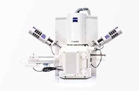
With ZEISS Crossbeam you benefit from a 3D nano-workstation
Combine imaging and analytical performance of a field emission scanning electron microscope (FE-SEM) with the processing ability of a focused ion beam (FIB).
During milling, imaging or when performing 3D analytics, Crossbeam will speed up your FIB applications. Make the most of your 3D analytics with the new EDS module.
Decide on exploiting variable pressure capabilities with ZEISS Crossbeam 340. Or use Crossbeam 550 for your most demanding characterizations.
Enjoy more options with the large chamber now.
More Information
Highlights
Within ZEISS Crossbeam Family you have the choice between Crossbeam 340 or Crossbeam 550. Exploit the variable pressure capabilities of Crossbeam 340. Or use Crossbeam 550 for your most demanding characterizations and choose the chamber size, standard or large, that best suits your samples.
| ZEISS Crossbeam 340 | ZEISS Crossbeam 550 | |
|---|---|---|
| SEM | Gemini I VP optics – | Gemini II optics Tandem decel option |
| Chamber Size and Ports | standard with 18 ports | standard with 18 configurable ports or large with 22 configurable ports |
| Stage | 100 mm travel range in x/y | standard with 100 mm or large 153 mm travel range in x/y |
| Charge Control | Flood Gun Local Charge Compensation Variable Pressure | Flood Gun Local Charge Compensation – |
| Exemplified Options | Inlens Duo for sequential SE/EsB* imaging VPSE detector | Inlens SE and Inlens EsB* for simultaneous imaging SE/EsB* imaging large airlock for 8 inch wafers configure three pneumatically driven accessories simultaneously on the large chamber, e.g. STEM, 4-Quadrant-Backscatter detetor, and local charge compensation |
| Advantages | Maximum sample variety due to variable pressure mode, wide range of in situ experiments, sequential Inlens SE / EsB* imaging possible. | High throughput in analytics and imaging, high resolution under all conditions, simultaneous Inlens SE and Inlens EsB* imaging. |
| * SE secondary electron, EsB energy selective backscatter |


